Raycision Empowers Research and Industry with Imaging and Radiation Solutions Tailored to Your Exact Needs.

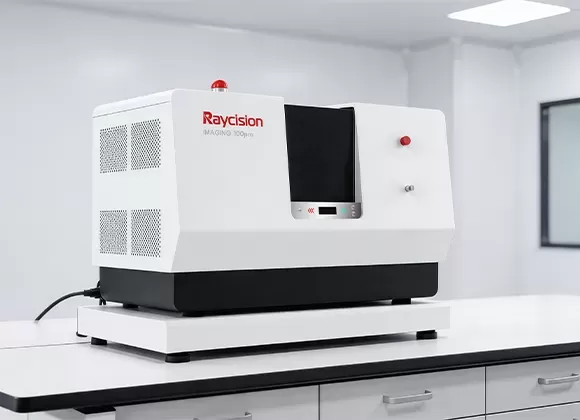

Industrial CT and non-destructive testing enable internal structure analysis and faster R&D and quality optimization. High-resolution imaging provides 3D visualization of defects and microstructures, while high-energy scanning supports reliable inspection of large, dense parts. Together, they enhance part integrity evaluation and improve manufacturing efficiency.
High-resolution 3D imaging reveals internal defects and microstructures without damaging samples.
Reliable inspection across electronics, EV batteries, casting, additive manufacturing, and aerospace.
Strong penetration enables stable imaging of thick and dense industrial components.
Combines imaging, measurement, and defect analysis to improve R&D and production efficiency.
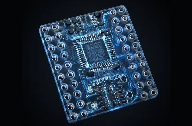 Semiconductor & ICs
Challenge: Detection of BGA and FC solder joint defects, including voids, non-wetting, opens, bridging/shorts, ball shift, deformation, and insufficient solder wetting.
Solution: 3D reconstruction and slice-by-slice inspection reveal hidden solder balls and detect voids, bridging, missing balls, and misalignment, with quantitative void ratio analysis.
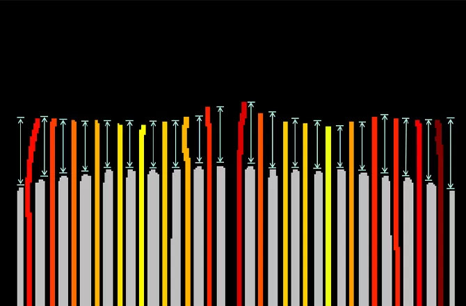 New Energy Batteries
Challenge: Detection of electrode misalignment in winding/stacking, metal contamination, improper tab overhang, and module welding defects.
Solution: 3D CT reconstruction visualizes internal electrodes and separators layer by layer, rapidly locates defects and inclusions, and measures tab overhang while detecting cold welds, cracks, and welding voids.
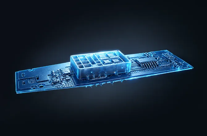 Consumer Electronics & PCBs
Challenge: Quality inspection of buried, blind, and through vias in multilayer PCBs, plus BGA/QFN solder defects such as voids, non-wetting, and bridging.
Solution: 3D reconstruction detects voids, wall cracks, and positional deviations in vias with dimensional measurement. Virtual CT slicing removes occlusion for rapid, quantitative solder defect inspection.
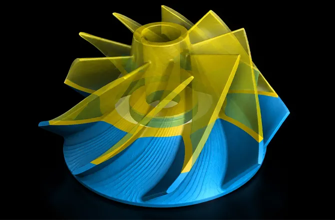 Aerospace Component Inspection & Metrology
Challenge: Detection of internal shrinkage, porosity, and thermal cracks in aerospace castings, plus complex internal structures in precision fluid components and pipelines.
Solution: 3D industrial CT detects micron-scale pores, porosity, and thermal cracks with quantitative defect measurement. Virtual sectioning enables non-contact dimensional inspection of internal cavities, burrs, residues, and flow-channel deformation.
Raycision Empowers Research and Industry with Imaging and Radiation Solutions Tailored to Your Exact Needs.