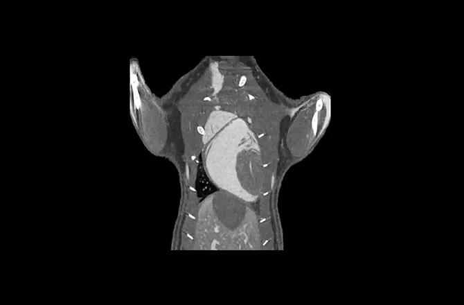
Software
AI-Driven Image Processing and Data Analysis
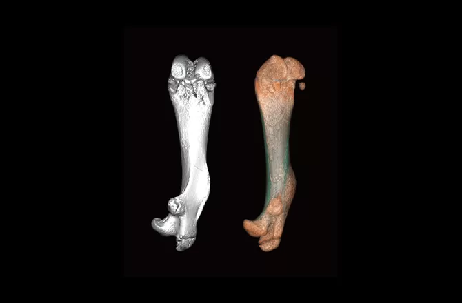
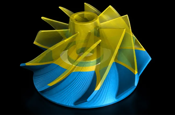
A multi-scale CT image intelligence platform for life sciences and industrial manufacturing
Learn More

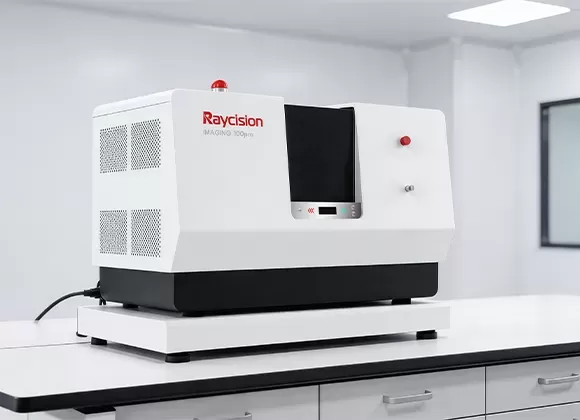
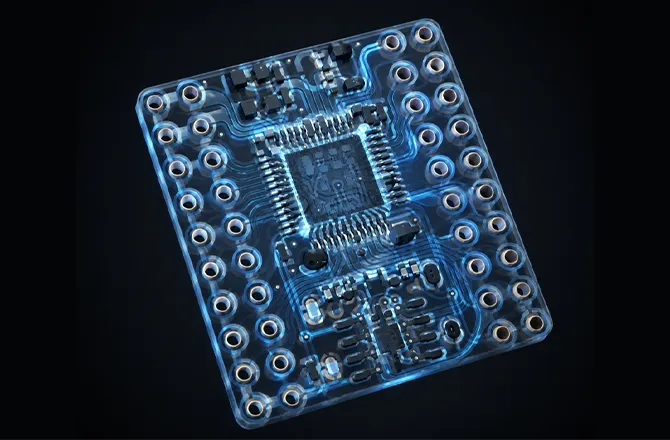
Industrial CT eliminates structural occlusion through non-destructive inspection, detecting hidden defects in PCB/PCBA layers and solder joints with 3D measurement for quality control and failure analysis.
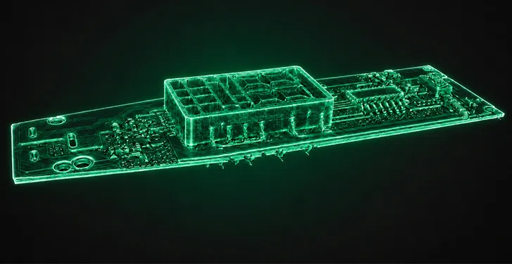
Industrial CT non-destructively removes occlusion from components and shielding layers, enabling 3D inspection and measurement of PCB/PCBA blind and buried vias, inner traces, solder joints, and underfill for defect detection, process optimization, and failure analysis.
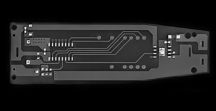
Virtual slicing eliminates the need for physical sectioning, enabling layer-by-layer inspection of blind/buried vias, inner traces, solder joints, and underfill for rapid defect localization and root-cause analysis.
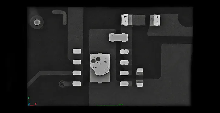
Porosity analysis non-destructively quantifies void volume, ratio, and distribution in PCB vias, solder balls, and underfill, supporting process evaluation and reliability assessment.

Raycision Empowers Research and Industry with Imaging and Radiation Solutions Tailored to Your Exact Needs.